Nanometer Thin Film thickness measurement is a crucial aspect of semiconductor manufacturing and research and development (R&D). It plays a vital role in providing feedback and optimization guidance for manufacturing processes, while also ensuring the performance and quality of semiconductor devices. Accurate measurement of Nanometer Thin Films is essential as these films are used in multiple layers within semiconductor devices, with each layer’s thickness directly affecting the device’s function and performance. Nanometer Measurement Methods are employed to guarantee that each layer adheres to design specifications, and they offer valuable insights into the manufacturing process, helping engineers to optimize production efficiency and improve device reliability. For more on semiconductor manufacturing, check out resources from the Semiconductor Industry Association, which provides comprehensive data and trends in the semiconductor field.
1. Electron Microscope Method
Principle: The electron beam emitted from the electron gun passes through the condenser lens and is focused into a narrow, bright, and uniform spot, which irradiates the sample inside the sample chamber. The electrons passing through the sample carry structural information about the sample. The dense areas of the sample let fewer electrons pass through, while the sparse areas let more electrons through. After being focused and magnified by the objective lens, the electron beam enters intermediate lenses and the 1st and 2nd projection lenses for further magnification, eventually projecting the enlarged electron image onto a fluorescent screen in the observation chamber. The fluorescent screen converts the electron image into visible light for the user to observe.
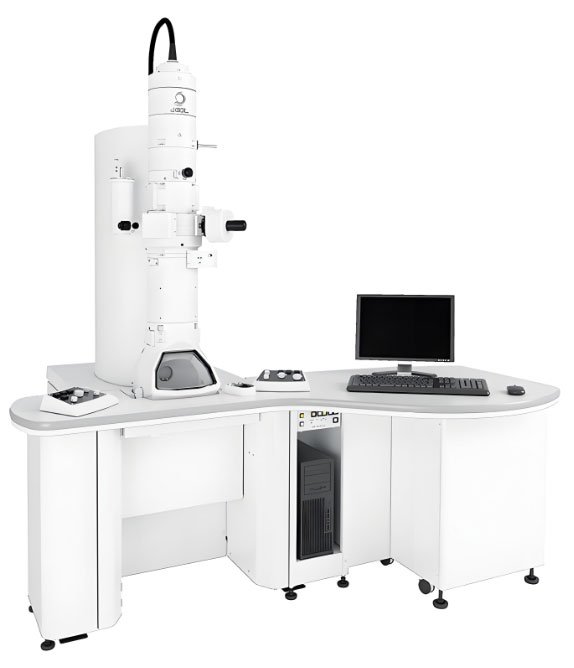
Detection Equipment: Scanning Electron Microscope (SEM), Transmission Electron Microscope (TEM)
Common Standards:
- GB/T 20307-2006: General rules for scanning electron microscope measurement of nanometer-level length
- ASTM B748-90(2021): Method for measuring metal coating thickness using scanning electron microscope
- GB/T 16594-2008: General rules for scanning electron microscope measurement of micron-level length
- GB/T 17722-1999: Scanning electron microscope measurement method for metal coating thickness
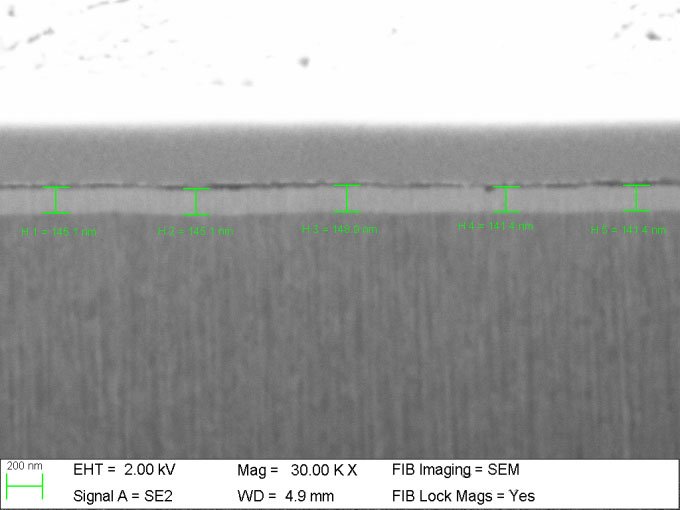
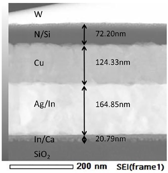
Test Case:
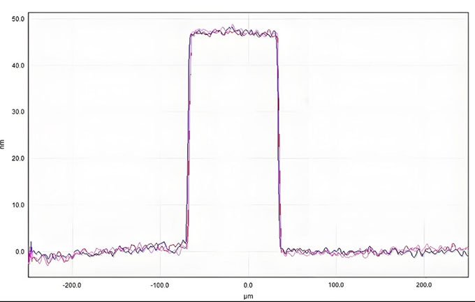
2. Profilometer Method
Principle: The profilometer method, also known as the contact method, involves using pre-coated or post-dissolution techniques to remove the coating in certain areas of the substrate. This creates a step between the substrate and the coating. When the probe of the profilometer passes over this step, the height of the step (i.e., the coating thickness) can be determined by measuring the movement of the probe and electrical signals. This method can measure coating thickness over a broad range from 0.01 to 1000μm, with an error margin within ±10%.
Detection Equipment: Step Gauge
Common Standards:
- GB/T 11378-2005: Measurement of metal coating thickness using the profilometer method
- GB/T 33826-2017: Measurement of nanofilm thickness on glass substrates using the stylus profilometer method
Test Case:
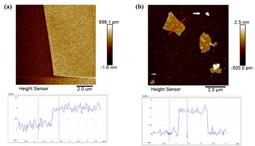
3. Atomic Force Microscopy Method (AFM)
Principle: Atomic Force Microscopy (AFM) is a tool used to study the surface structure of solid materials, including insulators. It works by detecting the extremely weak atomic interactions between the sample surface and a micro force-sensitive probe to analyze the surface structure and properties of the material.
Detection Equipment: AFM
Common Standards:
- GB/T 40066-2021: Measurement of graphene oxide thickness using AFM
- GB/T 40128-2021: Surface chemical analysis of material thickness using AFM for molybdenum disulfide layer materials
Test Case:
Measurement Equipment: